Nanobubbles penetrate deep into small crevices to dislodge and remove contaminants and sludge particles from the surface of the wafers.
Nanobubbles reduces mechanical stress to minimize damage to chips and improves the overall yield and quality of the dicing process.

Nanobubbles increase heat transfer properties. Cooler tools for extended life, and cooler workpiece for more precise dicing.
Nanobubbles reduce surface tension of cleaning solutions for increased tool life and decrease damage to chips.

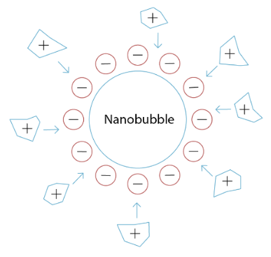
Nanobubbles Increased zeta-potential attracts and collects opposite charged sludge particles and better penetrates boundary layers on opposite charged surfaces.
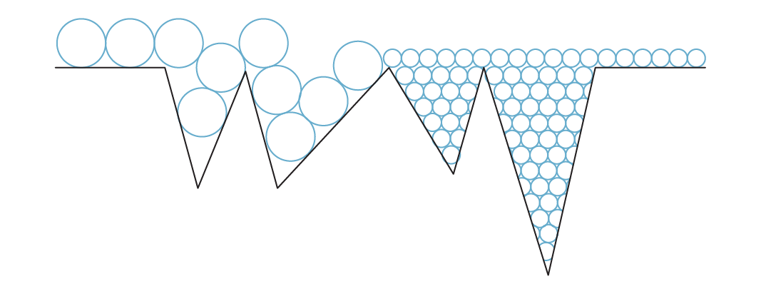
The small size of nanobubbles allows them to penetrate into small cracks, crevices, and pores that larger bubbles or conventional cleaning methods might miss. This ensures thorough cleaning and removal of stubborn residues.
Nanobubbles have a strong negative surface charge that enables them to absorb positively charged dirt and oily contaminants floating in the water.